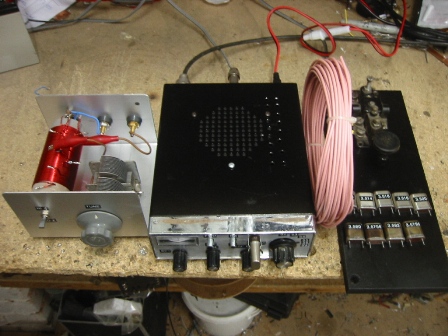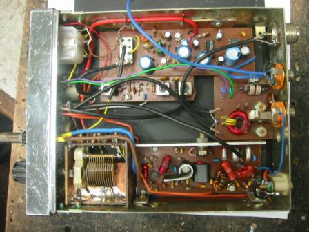
This transceiver came about from wanting something reasonably small and simple to use on camping holidays. Despite its simplicity performance is very good and has provided many very enjoyable CW qso’s. The receiver section comprises of a direct conversion receiver with a ceramic resonator VXO covering approximately 3.5Mhz to 3.6 MHz, stability/drift is very good after an initial warm period of ten minutes or so. The transmitter section is crystal controlled and provides just over five watts power output depending on crystal activity. A simple SWR bridge is also incorporated in the transmitter. The transceiver is built into an old CB radio case; all controls are on the front panel along with a crystal socket for the transmitter crystal.
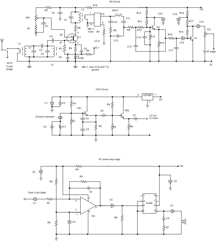
The receiver section is comprised of a dual gate mosfet RF preamp, a double balanced diode ring mixer, an active low pass audio filter, AF preamp and power amp stage. The mixer local oscillator injection is provided by the VXO. RF signals are coupled to Tr1 gate one via a band pass filter T1, T2, C1, C2 and C3. The gain of Tr1 is controlled by it’s gate two voltage via Vr1. Tr1’s source and gate one sit at roughly two volts due to LED1/R5, this allows the gate two to go negative with respect to source giving a much greater gain range, the more usual method where g2 volts goes down to zero volts with the source at a volt or so only gives about 10dB gain reduction whereas using the LED allows the FET to be completely cut off. Tr1 stage is included to make up for the insertion loss of the mixer and to improve front end sensitivity. T3 is a tuned drain load for Tr1, the low impedance secondary provides a good match to the mixer ( SBL-1 ) RF input. The local oscillator signal is injected into pin 8 of the mixer. Audio and RF frequencies are present on pin 3, 4 (I.F. output) of the mixer, this port is terminated at RF by C10/R8. RF is blocked by RFC1 thus only AF are passed to TR2 stage; an active low pass filter. The turnover frequency of this filter is roughly 1KHz. It is this stage that determines the selectivity of the receiver, under very crowded band conditions a high slope bandpass filter would be better suited here but for general use the low pass filter is sufficient. Tr3 is configured as an AF preamp the output of which is fed to the volume control and then to another preamp comprising of a 741 op amp and then on to the AF power amp; a LM386. The audio gain was divided amongst these three stages to provide stability, I did try using the LM386 on its maximum gain configuration without the 741 but it proved very unstable, it would break into oscillation and make all sorts of strange noises. Using several lower gain stages cascaded to achieve the total gain required gave excellent stability. Circuit diagram in pdf format

The VXO is fairly straight forward, Tr1, X1 and its associated components form the variable frequency oscillator. Tr2 is used as a buffer stage to drive the low impedance input of the mixer; this stage greatly aids the stability of the VXO oscillator. Vc1 is used as the tuning control, roughly 100 KHz tuning range is achieved with this circuit, and however some variations may occur depending on the ceramic resonator used so experimentation may be needed here. A friction reduction drive is used with Vc1.
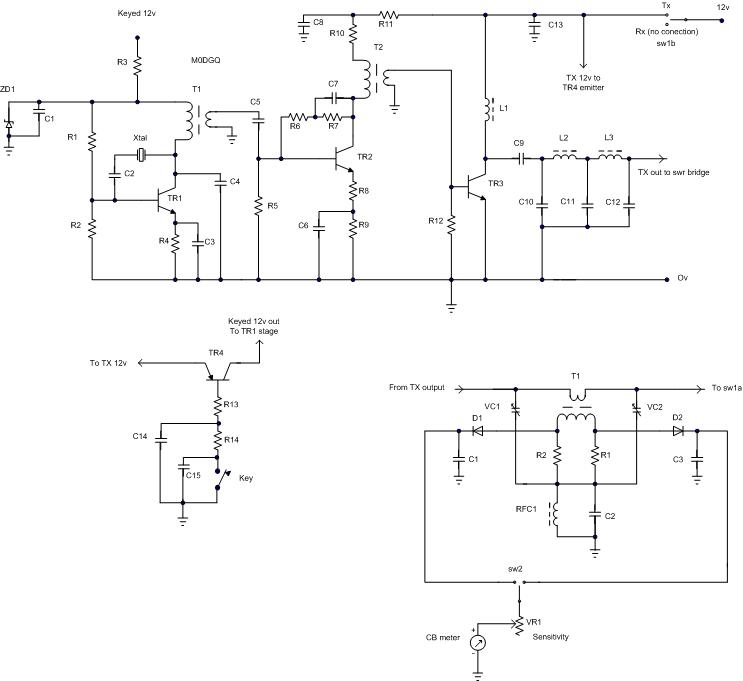
The transmitter section comprises of three stages; a Pierce crystal oscillator, a buffer amplifier and the power amplifier. The crystal oscillator is keyed via Tr4 a PNP transistor. Tr1 is configured as a Pierce oscillator; T1 and C4 form a tuned collector load. T1 secondary provides a good impedance match to Tr2 base. Tr2 is used as a buffer/amplifier; it gives isolation to the oscillator from the following stages and also raises the oscillator output level suitable to drive Tr3 to five Watts output. Shunt feedback and emitter degeneration is used in Tr2 to give a predictable amount of gain and stability. T2 forms an untuned collector load for Tr2, T2 secondary provides a suitable impedance match to Tr3 base. Tr3 is biased in class C making it a very efficient output stage. L1 is the collector load for Tr3 which feeds the pie low pass output filter. One half of a double pole changeover switch is used for antenna switching between the receiver and transmitter, the other half applies 12 volts to the transmitter when in the Tx position (SW1 a and b). With a 12 volt supply, power output from this transmitter is a little over five Watts with any of the crystals I have for this set. The note produced is very pleasant, no chirp is detectable. In the prototype I used the output transistor from a Pye Europa PMR set, a CB output transistor should be fine although I have not tried this yet. No side tone oscillator is necessary as the receiver is always on, when transmitting you will hear your actual carrier (be sure to turn the Rx volume down before transmitting). A simple SWR bridge is incorporated in the set, I take no credit for this SWR bridge design as it came straight out of the ARRL handbook. Circuit diagram in pdf format

There are several cheap common crystals available within the CW portion of 80M; 3.5795 (American colour burst), 3.560 QRP calling, 3.5879 , 3.5756 and 3.5820 are a few ( G-qrp club ). Rallies are a good source also, if you like rooting around in the junk piles.
The receiver is capable of resolving signals in the 0.5uV region so it is very sensitive but a good aerial should be used to make the most of the five watts qrp. When portable I usually use a half wave long wire with an L – match, this combination has always yielded good results, inter-G and European QSO’s have been had with ease.
T1, T2 and T3 rewound CB type IF transformer, primary 4 turns, secondary 28 turns. C1, 3, 220pf. C2, 22pf . C4, 1nf. C5, 12, 1nf. C7, 150pf. C8, 9, 6, 100nf. C10, 10nf. C11, 4n7. C13, 14, 17, 22nf. C15, 16, 1000uF. C18, 19 1uF. R1, R5, 1k. R2, 6k8. R3 , 15k. R4, 270. R6, 47. R7, 27. R8, 47. R9,10,15, 10k. R11, 13 220k. R12, 18, 1k2. R14, 2k2. R16, 1M5. R17, 5k6. R18, 150. VR1, 10k lin. VR2, 10k log. Tr1, BF981 etc. Tr2, 3, BC108. Diode ring mixer = SBL-1.
C1, 10uF. C2, 100nF. C3, 15pF. C4, 400pF. C5, 200pF. C6, 100pF. C7, 1nF. VC1, 100pF. R1, 2, 22k. R3, 1k5. R4, 15k. R5, 10k. R6, 330. Tr1, 2, BC108. Reg1, LM7808. Resonator = 3.58MHz ceramic resonator.
C1, 5, 1uF. C2, 6, 1000uF. C3, 10uF. C4, 330pF. C7, 220uF. C8, 100nF. R1, 6, 10k. R2, 3, 15k. R4, 220k. R5, 1k. R7, 4R7 Ic1, 741 op amp. Ic2, LM386.
R1, 15k. R2, 5k6. R3, 150R. R4, R12, 100R. R5, 1k2. R6, 560R. R7, 3k3. R8,4R7. R9, 18. R11, 47R. R13, R14, 1k. C1, C3, C6, C7, C8, C13, 100nF. C2, C4, C12, 1nF. C5, C9, C14, C15 10nF. C10, 800pF. C11, 1.5nF. Tr1, bc108. Tr2, 2n3866. Tr3, Europa output transistor, or try 2sc1969, 2sc2166 etc. Tr4, bc557. ZD1, 8v2. L2, 3, 24 turns 26SWG enamelled Cu on T50-2.
D1, D2, 1N4148. C1, C2, 10nF. VC1, VC2, 30pF. C2, 270pF. RFC1, 1mH. T1,Pri 60t 32 swg enameled Cu, Sec 3t pvc hookup wire on T68-2 core. R1, R2, 27R. VR1, 10k lin.


Barry Zarucki M0DGQ